Conference Introduction

Since Nanoimprinting technology was invented in 1995, it has completed 30 years of technological development. Because of its excellent technical characteristics—high resolution, low cost, and high productivity—it was considered a star technology at its birth. It has been rated as "one of 10 emerging technologies that will change the world" (MIT Technology Review), receiving extensive attention from academia and industry and even being included in the international semiconductor industry technology development blueprint.


The development of nanoimprint technology is not only the result of academic progress but also the industry's contributions. While receiving extensive attention in the academic field, nanoimprint technology has also entered the industrial market. The continuous development and commercialization of nanoimprint technology have been driven by key players such as Nanonex, Obducat, and Molecular Imprint, all of which have made significant contributions. Later, Suss and EVG also contributed greatly to the industrialization of nanoimprint technology.


Especially in recent years, China's industrial demand for large-volume, high-precision micro- and nano processing has exploded. This demand is evident in various application areas, including micro- and nano optical components, AR lenses, DOE, TOF, and MLA. Moreover, in biomedical applications such as biochips, microfluidic channels, and microneedles, nanoimprint technology shows great potential. A large number of high-tech start-up companies have emerged in these fields, and some large listed companies have also started to explore nanoimprint technology, investing huge amounts of funds and resources. They are actively pushing the industrialization of nanoimprint technology to a new level in China.


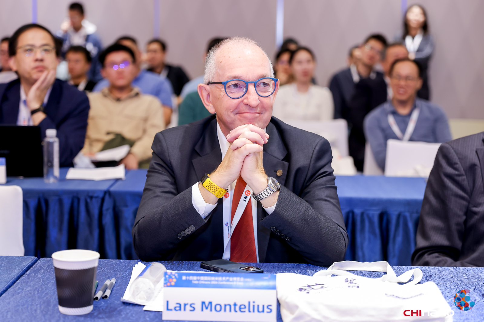
In 2023, Chinese experts in the field of nanoimprint technology hosted the first NTAC Global Nanoimprint Technology and Application Conference in Suzhou, providing a long-term and stable communication platform for the research and industry community committed to nanoimprint technology development. The first NTAC conference invited a large number of experts and scholars in the field of nanoimprint to discuss cutting-edge technologies and exchange the latest achievements, sparking a warm response. The 2nd NTAC Global Nanoimprint Technology and Application Conference in 2024 assembled an impressive lineup of keynote speakers, including: Professor Zhou Yu from Princeton University, widely regarded as the "Father of Nanoimprint Technology"; Professor Lars Montelius from Lund University, Sweden, one of the pioneers of nanoimprint technology and others. A total of 21 leading experts and industry representatives from around the world engaged in in-depth discussions on the latest advancements and applications of nanoimprint technology. The NTAC Conference not only established a cutting-edge communication platform between academia and industry in the field of nanoimprint technology, facilitating profound dialogues among experts and scholars but also outlined a clear roadmap for the future development of the industry.


In 2025, marking the 30th anniversary of the invention of nanoimprint technology, the 3rd NTAC Conference—30 Years of Nanoimprint Celebration Special—will be grandly held in Suzhou in the golden autumn of October. Hosted by Gusu Lab and organized by Suzhou New Dimension Nano Technology Co., Ltd., the conference will integrate top industry resources, focus on nanoimprint technology innovation, and strive for industrial co-construction and win-win development. It will feature discussions on cutting-edge hotspots and research achievements in the field of nanoimprint, aiming to accelerate breakthroughs in the development bottlenecks of nanoimprint technology manufacturing and contribute to technological innovation and industrial development of domestic manufacturing.

Conference Organizers

Organization

Host

    • Gusu Lab

Organizer

    • Suzhou New Dimension Nano Technologies Co., Ltd.

Co-organizer

    • Nanopolis Suzhou Co., Ltd.

Main topics

2025 Agenda Overview

2025 Agenda Overview

Date: Oct. 22
Location: A109, Suzhou International Expo Center
Moderator: Gang Luo,Professor of Gusu Lab, CEO of Suzhou New Dimension Nano-technologies Co., Ltd.
Date: Oct. 23, AM
Location: A109, Suzhou International Expo Center
Date: Oct. 23, PM
Location: A109, Suzhou International Expo Center
The 3rd Global Nanoimprint Technology and Application Conference
Gang Luo
Professor of Gusu Lab, CEO of Suzhou New Dimension Nano-technologies Co., Ltd.
The 3rd Global Nanoimprint Technology and Application Conference
Lars Montelius
Professor Emeritus of Lund University, Former Director–General of the International Iberian Nanotechnology Laboratory, Founder of Obducat
Abstract of Speech:Professor Lars Montelius, one of the pioneers of nanoimprint technology, has been deeply engaged in the field of nanotechnology for 30 years. His work centers on lithography and processing technologies applied to various nanodevices, with a particular focus on the subfields of nanoimprint and lithography. He and his team have published a number of highly influential papers. To date, Prof. Lars Montelius has published more than 170 papers, given more than 80 invited lectures and filed 54 patents., leaving a profound academic mark in the nanoscience and technology community. From 2003 to 2009, he served as Head of the Department of Physics at the Faculty of Science and Engineering, Lund University, demonstrating outstanding academic leadership. During 2009-2011 he was the director for the Øresund University & Øresund Science Region, a cross-border cooperation between eleven universities, three regional authorities, two countries in the Øresund Region, and led the organization to achieve numerous outcomes. Between 2007 and 2014, he was Chair of the Swedish Technical Standardization Committee on Nanotechnology, making important contributions to the standardization process in the field of nanoscience and technology. Since September 1, 2014, Professor Lars Montelius has served as Director of International Iberian Nanotechnology Laboratory in Braga, Portugal. Prof. Lars Montelius is also a former President of the International Federation for Vacuum Science Technology and Applications (国际真空科学技术与应用联盟), one of the decision-makers of the EU NMBP (Nanotechnology, Advanced Materials, Biotechnology and Processing) Expert Group, and a member of the Board of Directors and Head of the Working Group of the two major European technology platforms, NANOFutures and EuMat.
Biography of the Speaker:Semiconductors power virtually all modern technologies — from smartphones and AI data centers to electric vehicles (EVs), industrial automation, and medical devices. As more industries digitize and automate, the need for advanced chips grows. AI Boom: Training and running large AI models (like ChatGPT) require massive computational power, driven by GPUs and AI-specific chips. EV & Mobility Shift: Electric and autonomous vehicles need significantly more chips than traditional cars — for sensors, power management, infotainment, etc. IoT Growth: Billions of devices (smart homes, factories, etc.) are connecting to the internet, all requiring semiconductors. The COVID-19 pandemic and geopolitical tensions exposed the fragility of the global chip supply chain, making us aware of the necessity of robust supply chains – and today we witness the resulting increased demand for national manufacturing capabilities of critical products. In addition, there is a worldwide increased political instability. Semiconductors – and the semiconductor fabric is a driver for nearly every modern technology that in turn is driving our society at large. Semiconductors are now considered strategic assets — much like oil in the 20th century. Nanotechnology is a Key Enabling Technology with promises for making solid contributions to the grand societal challenges of today, offering possibilities to address solutions for enabling sustainable energy supply on demand, clean water to everyone, novel e-care and e-health paradigms etc. Nanoimprint lithography has since its inception 30 years ago quickly developed from the R&D stage to the present industrial state-of-play. The NIL technology is now considered to be one of the most prominent enabling technologies for applications in the most important fields for sustainable societal development, spanning from optics (eg. AR,VR, displays), electronics (eg. energy efficient AI, quantum devices and sensors), electrification (eg. EVs, energy harvesting/storage) to biotech and medical (eg. biosensors, DNA-chips) fields. Further, the inherent enabling character of NIL technology, provides it to have a large transformative potential with huge implications for a sustainable societal development. These major societal developments challenge the present higher education systems, the industrial society as well as the society-at-large. There will be an increased demand for transversal interdisciplinary participation to enable the needed disruptive innovations to happen. Presently there are urgent needs for novel solutions and incentives to recruit needed trans-disciplinary engagements and closer collaboration with the industrial fabric - as well as with society at large. Simply put, there is a need to join forces to create a global systemic and inclusive Science, Technology, Society and Innovation pathway for People, Planet and Prosperity.
The 3rd Global Nanoimprint Technology and Application Conference
Stephen Y. Chou
Joseph C. Elgin Professor at Princeton University
Biography of the Speaker:Stephen Y. Chou is the Joseph C. Elgin Professor at Princeton University. He is the founder and founding chairman of the board of three startup companies: Nanonex Corp., NanoOpto Corp., and Essenlix Corp., and a co-founder of BioNano Genomics Inc. Among other awards and honors, he is a member of the US National Academy of Engineering (2007), a Fellow of the US National Academy of Inventors (2013), and a recipient of the IEEE Cledo Brunetti Award (2004), the IEEE Nanotechnology Pioneer Award (2014), and the Nanoimprint Pioneer Award (2015). He is also a Packard Fellow (1990), and a Fellow of the IEEE (2000), the American Vacuum Society (AVS) (2010), the Optical Society of America (OSA, now Optica) (2011), and the International Society for Nanomanufacturing (ISNM) (2010), and an inductee of the New Jersey High Tech Hall of Fame (2004). He was twice recognized by MIT Technology Review for his technologies as one of the "Ten Emerging Technologies That Will Change the World": in 2003 (nanoimprint) and in 2007 (nanochannel for DNA sequencing, mapping, and manipulation). Over the past four decades, Chou's pioneering research has spanned several fields, including nanofabrication, a broad spectrum of nanodevices (electrical, optical, magnetic, and biological) and their applications, bioengineering, and medical diagnostics. His groundbreaking inventions, pioneering works and vision, and entrepreneurship have dramatically reshaped and advanced their fields; created multiple new research fields and areas, launched new industries, been broadly adopted across numerous disciplines and industrial sectors, generated multi-billion-dollar businesses, transformed both academia and industry, and profoundly benefited the economy and society. Chou is acclaimed as the father of nanoimprint, having created the field with his 1995 invention, revolutionized nanopatterning, nanomanufacturing, and industrial applications, and founded the first nanoimprint company, Nanonex, in 1997. He is also regarded as the father of nanoimprint applications, being the first to use it for fabricating electrical, optical, magnetic, and biological nanodevices, and he founded NanoOpto, the first company to produce subwavelength optical elements ("meta optics") using nanoimprint. Moreover, Chou is recognized as the father of iMOST (instant Mobile Self-Test), a revolutionary diagnostic platform that provides instant, laboratory-accurate results anywhere, anytime, by nearly anyone, even under imperfect conditions. He founded Essenlix (2013), the first company to commercialize this technology. Additionally, Chou is known for his pioneering work in scaling transistors to new regimes, notably the first crystalline Si room-temperature single-electron transistor (1996) and the first GAA (Gate-All-Around) nano-transistor in 1997. Chou’s other work includes the invention and pioneering of various electronic, optical, magnetic, and biological nanodevices with unique properties, as well as various new nanopatterning methods, including lithographically induced self-assembly (LISA), self-perfection by liquefaction (SPEL), and laser-assisted direct imprint (LADI). Chou has authored over 700 refereed journal and conference papers (H-index = 97, ~44,000 citations), and has delivered over 230 plenary and invited talks. He is the primary inventor and author of over 400 patents and applications, with more than half granted. According to Google Patents, Chou’s technologies have been referenced in over 60,000 granted and pending patents worldwide. Chou has served over 150 times as a Conference Chair, Co-chair, Program Chair, Steering/Advisory Committee member, and Session Chair.
The 3rd Global Nanoimprint Technology and Application Conference
Yifang Chen
Professor of Fudan University
Abstract of Speech:On the 30 years’ anniversary of the great invention of nanoimprint lithography (NIL) by Prof. Stephen Chou, this talk will first give some statistics of the overall fundamental research and technical development in China in the past three decades. Then, the talk will give a short review of some researches and achievements at Fudan University in NIL, which were conducted in the period of 2006-2012 in the international collaboration with Rutherford Appleton Laboratory in the UK. Particularly, nanoimprint processing study on epoxy resin such as SU-8 was systematically carried out for duplication of templates, imprint mechanism, imprint parameter optimization, device fabrication, characterization and applications. Over 37 related SCI-articles were published as the milestone of the pioneering work by Fudan University at early-stage development of nanoimprint lithography in China.
Biography of the Speaker:Prof. Yifang Chen received his D.Phil degree in Condensed Matter Physics from University of Oxford, UK, in 1995. He was a postdoctoral researcher in Delft University of Technology, the Netherlands (1994-1996), Nanyang Technological University, Singapore (1996), and University of Glasgow, UK (1997-2002). From 2003 to 2012, he became a senior and then principal scientist of Nanotechnology in Rutherford Appleton Laboratory, UK; he was a visiting professor at École Polytechnique Fédérale de Lausanne (EPFL), Switzerland (2010) and visiting senior scientist at National Physical Laboratory (NPL) UK (2016-2019). In 2012, he joined Fudan University through national high-end talent plan and received a special government allowance of the State Council in 2018. Dr. Yifang Chen has been dedicated in the fundamental researches of nanofabrication and applications since 1990, applying processes such as electron beam lithography / nanoimprint /dry-etch for fields spanning novel nano-photoelectronic devices and chips, InP-based high-electron transistors (HEMTs), development of key optical components for X-rays, polarizers and vortex beam manipulation devices based on metasurface material, and two-dimensional nano-photonic crystals, among others. Especially in the development of key optical components for X-ray nanomicroscopes, he has led his team to fill the gap in the country by manufacturing a novel X-ray lens with 15 nm resolution, which marks his research in the world leading position. He has published more than 150 SCI papers and awarded 10 national patents. He is the associate editor-in-chief of Microelectronics Engineering (Elsevier) remote referee of European Research Council (ERC), etc.
The 3rd Global Nanoimprint Technology and Application Conference
Helmut Schift
Head of Advanced Nanomanufacturing (ANaM) Group in PSI
Abstract of Speech:Switzerland has a long tradition in polymer replication techniques, due to its security industry fabricating counterfeit features for banknotes and identity documents such as passports. Apart from holograms, laser writing techniques were developed at the Zürich branch of Paul Scherrer Institute (PSI), as a Swiss national institute. When I was coming from Mainz in Germany to PSI in 1994, I had a background in LiGA technology, a microtechnology based on lithography, electroplating and molding. In 1997, I submitted my first project proposal about NIL, and consequently, independent from European projects, we established basic knowledge about polymer rheology of thin films using NIL. For me, nanoimprint was simply a downscaling of micro-embossing, and therefore we called it hot embossing lithography. My first real NIL paper, with sub-100 nm resolution imprinting in PMMA and pattern transfer, was on “Hot embossing in polymers as a direct way to pattern resist”, presented at the Micro- and Nanoengineering (MNE) conference in 1997 and published in Microelectronic Engineering (MEE) in 1998. PSI was joining the large European project NaPa (2004-2008) and NaPANIL (2008-2012). NaPa included dissemination activities such as the NaPa Summer school at the University of Toulouse and the NaPa library of processes.
Biography of the Speaker:Helmut Schift studied electrical engineering at the University of Karlsruhe, and performed his Ph.D. studies at the Institute of Microtechnology Mainz (IMM), Germany. He has specialized in micro-optics, high aspect ratio lithography and polymer replication (LiGA technology). After his graduation in 1994, he joined the Paul Scherrer Institute as research staff member, where he has subsequently built up and established a technology platform for nanoimprint lithography (NIL). As one of the pioneers, H. Schift developed enabling techniques for the patterning of functional surfaces with topological and chemical surface contrast, and used these processes in different research and application fields. Since 2001, he is Lecturer at the University of Applied Sciences and Arts (Fachhochschule) Nordwestschweiz for engineering students on “Micro- and Nanotechnology”. In 2002, he became head of the Polymer Nanotechnology Group (INKA-PSI). During a sabbatical in 2011, he was employed as a visiting professor (Velux grant) in the Optofluidics group in the Department of Micro- and Nanotechnology at the Danish Technical University (DTU). H. Schift is a co-author of 140 scientific papers, including reviews and book chapters, and editor of the NaPa Library of Processes. He has supervised many scientific projects and participated in several PhD juries. In the European FP7 NaPANIL project (2008-2012), H. Schift was sub-project leader with over 1000 person months. He received the Swiss Technology Award (2005, Sonderpreis Ostschweizer Kantone) and Nanoimprint Pioneer Award (2016). In 2016 he was recognized by the AVS Journal of Vacuum Science and Technology as one of its Most Valuable Reviewers. Since 2019, H. Schift is Consultant on Research Integrity (30%) at PSI. For this purpose, in 2021, he completed MAS studies of Applied Ethics at the University of Zürich.
The 3rd Global Nanoimprint Technology and Application Conference
Gang Luo
Professor of Gusu Lab, CEO of Suzhou New Dimension Nano-technologies Co., Ltd.
The 3rd Global Nanoimprint Technology and Application Conference
Feng Luo
Chair Professor of College of Materials Science and Engineering, Nankai University
Abstract of Speech:In this presentation, we will introduce photoresist combined with several MEMS process for optical applications. The combination of mask mold control and multiple etching techniques enables the fabrication of multilayer patterns across different materials, further expanding the versatility and potential applications of NIL.
Biography of the Speaker:Feng Luo, Chair Professor, College of Materials Science and Engineering/School of Electronic Information and Optical Engineering, Nankai University Feng Luo is currently a Chair Professor at College of Materials Science and Engineering, Nankai University, and Adjunct Chair Professor at Xi'an Jiaotong University (2018-2020). He received his B.S. and Ph.D. degrees from College of Chemistry and Molecular Engineering, Peking University, from 1995 to 2004. From 2004 to 2009, he worked as a postdoctoral fellow in Germany and Switzerland, and from 2009 to 2010, he was a PI Distinguished Fellow at College of Engineering. From 2010 to 2020, he worked at IMDEA Materials Institute, where he served as an associate researcher, researcher, and then tenure-track senior research professor. Since 2020, he has been working at Nankai University, where he has been selected into Marie Skłodowska-Curie Individual Fellowships, Outstanding Young Talents Fund of Spain, Outstanding I3 Professor of Spain, and the Fifteenth Key Talent Program of China. Currently, he is a member of Institute of Advanced Science Facilities, Shenzhen, consultant of Shenzhen Industrial Light Source, member of Shanghai Light Source, and Director of Lanzhou Institute of Aeronautical Integrated Circuits and Materials.
The 3rd Global Nanoimprint Technology and Application Conference
DaWei Wang
President of Shenzhen Micro-Nano Manufacturing Industry Promotion Associa
Abstract of Speech:Since 2018, the Promotion Association has continuously tracked the industrialization process of micro-nano imprint technology globally, especially in China. It has released multiple issues of the Industrialization Research Report on Nanoimprint Technology (Patents) and more than ten observation articles, building a communication bridge between nanoimprint enterprises, investment institutions, and application clients. In this speech, the Promotion Association will share several insights on the industrialization of this technology gained from its observation and research.
The 3rd Global Nanoimprint Technology and Application Conference
Lars Montelius
Professor Emeritus of Lund University, Former Director–General of the International Iberian Nanotechnology Laboratory, Founder of Obducat
Abstract of Speech:Professor Lars Montelius, one of the pioneers of nanoimprint technology, has been deeply engaged in the field of nanotechnology for 30 years. His work centers on lithography and processing technologies applied to various nanodevices, with a particular focus on the subfields of nanoimprint and lithography. He and his team have published a number of highly influential papers. To date, Prof. Lars Montelius has published more than 170 papers, given more than 80 invited lectures and filed 54 patents., leaving a profound academic mark in the nanoscience and technology community. From 2003 to 2009, he served as Head of the Department of Physics at the Faculty of Science and Engineering, Lund University, demonstrating outstanding academic leadership. During 2009-2011 he was the director for the Øresund University & Øresund Science Region, a cross-border cooperation between eleven universities, three regional authorities, two countries in the Øresund Region, and led the organization to achieve numerous outcomes. Between 2007 and 2014, he was Chair of the Swedish Technical Standardization Committee on Nanotechnology, making important contributions to the standardization process in the field of nanoscience and technology. Since September 1, 2014, Professor Lars Montelius has served as Director of International Iberian Nanotechnology Laboratory in Braga, Portugal. Prof. Lars Montelius is also a former President of the International Federation for Vacuum Science Technology and Applications (国际真空科学技术与应用联盟), one of the decision-makers of the EU NMBP (Nanotechnology, Advanced Materials, Biotechnology and Processing) Expert Group, and a member of the Board of Directors and Head of the Working Group of the two major European technology platforms, NANOFutures and EuMat.
Biography of the Speaker:Semiconductors power virtually all modern technologies — from smartphones and AI data centers to electric vehicles (EVs), industrial automation, and medical devices. As more industries digitize and automate, the need for advanced chips grows. AI Boom: Training and running large AI models (like ChatGPT) require massive computational power, driven by GPUs and AI-specific chips. EV & Mobility Shift: Electric and autonomous vehicles need significantly more chips than traditional cars — for sensors, power management, infotainment, etc. IoT Growth: Billions of devices (smart homes, factories, etc.) are connecting to the internet, all requiring semiconductors. The COVID-19 pandemic and geopolitical tensions exposed the fragility of the global chip supply chain, making us aware of the necessity of robust supply chains – and today we witness the resulting increased demand for national manufacturing capabilities of critical products. In addition, there is a worldwide increased political instability. Semiconductors – and the semiconductor fabric is a driver for nearly every modern technology that in turn is driving our society at large. Semiconductors are now considered strategic assets — much like oil in the 20th century. Nanotechnology is a Key Enabling Technology with promises for making solid contributions to the grand societal challenges of today, offering possibilities to address solutions for enabling sustainable energy supply on demand, clean water to everyone, novel e-care and e-health paradigms etc. Nanoimprint lithography has since its inception 30 years ago quickly developed from the R&D stage to the present industrial state-of-play. The NIL technology is now considered to be one of the most prominent enabling technologies for applications in the most important fields for sustainable societal development, spanning from optics (eg. AR,VR, displays), electronics (eg. energy efficient AI, quantum devices and sensors), electrification (eg. EVs, energy harvesting/storage) to biotech and medical (eg. biosensors, DNA-chips) fields. Further, the inherent enabling character of NIL technology, provides it to have a large transformative potential with huge implications for a sustainable societal development. These major societal developments challenge the present higher education systems, the industrial society as well as the society-at-large. There will be an increased demand for transversal interdisciplinary participation to enable the needed disruptive innovations to happen. Presently there are urgent needs for novel solutions and incentives to recruit needed trans-disciplinary engagements and closer collaboration with the industrial fabric - as well as with society at large. Simply put, there is a need to join forces to create a global systemic and inclusive Science, Technology, Society and Innovation pathway for People, Planet and Prosperity.
The 3rd Global Nanoimprint Technology and Application Conference
L.Jay Guo
Professor of University of Michigan
Biography of the Speaker:L. Jay Guo is a Professor of Electrical and Computer Engineering at the University of Michigan. His is involved in interdisciplinary research, with activities ranging from polymer-based photonic devices and sensor applications, flexible transparent conductors, nanophotonics, structural colors and AI assisted design, hybrid photovoltaics and photodetectors, to nanomanufacturing technologies, and are contributed by students from Electrical Engineering and Optics, Macromolecular Science & Engineering, Applied Physics, Physics, and Mechanical Engineering. Prof. Guo has over 285 journal publications; with citation over 32,000 times, and an H-index of 89 (by google scholar). Some notable awards he received from recent years include 2023 Wise-Najafi Prize for Engineering Excellence in the Miniature World from University of Michigan, 2017 William Mong Distinguished Lecturer in Hong Kong University, and 2015 Monroe-Brown Research Excellence Award by the College of Engineering of University of Michigan. His professional service includes Associate Editor of Optica (till 2021); and currently member of the Editorial Advisory Board of Advanced Optical Materials, and Opto-electric Science. His entrepreneur activities include co-founding two startup companies to commercialize technologies from his lab.
The 3rd Global Nanoimprint Technology and Application Conference
Linsen Chen
Professor of Soochow University, Chairman of SVG Optronics
Abstract of Speech:Since Prof. Steven Chou proposed the concept of nanoimprint lithography (NIL) in 1995, research and development worldwide has exceeded 30 years. NIL has achieved significant technological breakthroughs and industrial applications in fields such as displays, optoelectronics, and biochips, demonstrating the advantages of high-throughput, high-precision, and low-cost nanomanufacturing. The report reviews the landmark progress made over the past more than twenty years, driven by the SVG team, in promoting the research and industrialization of NIL technology in China, including roll-to-roll (R2R) nanoimprint technology, large-area micro/nano mold fabrication, and influential industrial applications. It focuses on recent research work and application cases in roll-to-plate (R2P) alignment nanoimprint systems, low-deformation mold fabrication, and intelligent alignment processes. The report anticipates that the next five years will be an opportunity period for substantial breakthroughs in high-precision alignment NIL key technologies and equipment, with the potential for major applications in industries such as semiconductors and photonic chips, Light-field imaging and 3D displays, AR, biometric recognition, sensing, and meta-surface devices and meta-materials.
Biography of the Speaker:Dr. Chen is a Research Fellow and Doctoral Supervisor at Soochow University, as well as an expert receiving special government allowances from the State Council. He’s focused on the research and applications of micro-nano optics and flexible manufacturing, upstream materials and devices for new displays, and digital lithography & nanoimprint technology. He has presided over major projects including the National 863 Program, National Major Scientific Instrument and Equipment Special Project, and Key Projects of the National Natural Science Foundation of China. He has made systematic and pioneering contributions in areas such as 3D lithography technology and equipment, roll-to-roll nanoimprint technology and processes, micro-nano optical materials and devices, and new display technologies, with his research results widely applied at home and abroad. As the principal investigator, he has successively won 3 Second Prizes of the National Science and Technology Progress Award, 5 First Prizes of the Jiangsu Provincial Science and Technology Award, the Special Prize of the National "Award for Outstanding Individuals in Invention and Entrepreneurship" (and was awarded the title of "Contemporary Inventor"), and the 4th "Outstanding Engineer Award". He has published more than 190 papers in journals such as Light, PRL, Adv. Mater., EES, and Optica, and holds over 200 invention patents (7 have won the China Patent Excellence Awards). He is the founder of Suzhou SVG Tech Group Co., Ltd. (listed on the ChiNext Market) and currently serves as the chief scientist presiding over a National Key R&D Program project.
The 3rd Global Nanoimprint Technology and Application Conference
Michael Steigerwald
CEO of Raith Group
Abstract of Speech:RAITH is the global market and technology leader in maskless nanofabrication systems and characterization solutions. With our unique combination of high-precision products, integrated solutions, and proprietary technologies, we drive innovation and accompany a wide variety of industries and applications. In our speech „Mastering for Nanoimprint“ we introduce our company to the audience and present our solutions along the nanoimprint process from design to mass production. Focusing on mastering with electron beam- and laser beam lithography, automated 2D metrology and process control and potential 3D analysis methods.
Biography of the Speaker:Dr. Michael Steigerwald has a deep history in leadership roles, specifically within the field of nanotechnology and advanced scientific systems. He assumed the position of CEO at Raith Group, a global leader in nanofabrication and characterization systems. Raith has a strong reputation for innovation in critical industries such as semiconductor technology, quantum technologies, and materials science​. Before joining Raith, Dr. Steigerwald held a variety of management positions, most recently as Senior Director Engineering at US-based KLA, a leading manufacturer of wafer and reticle defect inspection systems for semiconductor production; prior to that he had been General Manager, Ion Microscopy Innovation Center, part of the scientific optics company Carl Zeiss in Peabody, USA, and Senior Manager Research & Development at Carl Zeiss NTS in Oberkochen, Germany.
The 3rd Global Nanoimprint Technology and Application Conference
Xin Cheng
Professor of Southern University of Science and Technology
Abstract of Speech:Nanoimprint lithography (NIL) is widely regarded as a strong candidate for next-generation lithographic techniques. After 30 years of reseach and development, nanoimprint is poised for commercial manufacturing of micro and nanoscale structures and devices for applications in optics, bioengineering, and electronics. At SUSTech, we adopt a holistic approach to develop nanoimprint technology. In this talk, we present our work on nanoimprint equipment and resist materials, and our efforts in defect mitigation. Applications of nanoimprint in optical and bioengineering applications will also be discussed. Finally, a discussion on the prospect of nanoimprint in electronic manufacturing is attempted through analyzing the unique strengths of nanoimprint as compared to conventional electron-beam and photolithography techniques.
Biography of the Speaker:Xing Cheng received his Ph.D. in Electrical Engineering from the University of Michigan in 2005. He previously served as Assistant Professor and Associate Professor in the Department of Electrical and Computer Engineering at Texas A&M University. Since 2013, he has been a professor in the Department of Materials Science and Engineering at the Southern University of Science and Technology (SUSTech), and was appointed Executive Dean of SUSTech’s College of Semiconductor (National Graduate College of Engineers) in 2024. His research and teaching focus on semiconductor materials, devices, and micro/nanofabrication, with interests spanning lithography, nanomanufacturing, microfluidic chips, and MEMS sensors. He has published over 140 journal articles and awarded more than 50 patents. He also led over 10 major research projects, including the National Natural Science Foundation of China’s Major Research Instrumentation Development Program and Guangdong Provincial Key R&D Initiatives, alongside 10+ industry collaborative R&D projects.
The 3rd Global Nanoimprint Technology and Application Conference
Yanxia Cui
Technical Expert of Huawei Technologies Co., Ltd.
Abstract of Speech:Nanoimprint Lithography (NIL) is a highly promising emerging technology in the semiconductor processing field. It not only boasts prominent advantages in low-cost, large-area pattern fabrication but also holds the potential for sub-10nm high-precision pattern manufacturing, providing a practical path to overcome the bottlenecks of traditional lithography technology. Currently, NIL has achieved large-scale application in mature fields such as anti-counterfeiting marks and CMF texture decoration. In emerging industries, it has also successfully realized mass production of key components including metal wire grid polarizers and AR waveguides. However, in the process of NIL-based mass production of high-precision optical structures like diffraction gratings, microlenses, and metasurfaces, there are still long-awaited technological bottlenecks to be broken through. This report will focus on sharing the key challenges faced by NIL technology as it currently enters semiconductor FAB production lines and enables the cross-domain integration and fabrication of optical and other functional devices.
Biography of the Speaker:Dr. Cui Yanxia serves as a Technical Expert in the field of Nanomanufacturing and Microdevices at the 2012 Advanced Manufacturing Laboratory of Huawei Technologies Co., Ltd. She graduated from the Optical Engineering major at Zhejiang University. She began working at Taiyuan University of Technology in 2011, was exceptionally promoted to Professor in 2013, and received approval for the National Excellent Young Scientists Fund in 2019. Since 2023, she has been with Huawei. She has also conducted academic visits to institutions including The Chinese University of Hong Kong, Hong Kong Baptist University and the University of Illinois at Urbana-Champaign (UIUC), USA. Her long-term research focuses on localized optical regulation of nanostructures and their applications in optoelectronic sensors. She has presided over 5 national-level projects (including one joint key project) and 14 provincial/ministerial-level projects, and won the Second Prize of Shanxi Provincial Natural Science Award. She has published 157 SCI-indexed papers (with 6,190 total non-self citations and 4 ESI Highly Cited Papers), obtained 30 authorized patents (including 3 international ones), and published one monograph. Additionally, she was selected into Elsevier's "China Highly Cited Researchers" list and has also received honors such as the Strong Nation Young Scientists Nomination Award, Huawei 2012 Labs Innovation Pioneer, and Huawei Central Research Institute President's Team Award.
The 3rd Global Nanoimprint Technology and Application Conference
Wanyin Cui
General Manager of Nanoscribe China Co., Ltd.
Biography of the Speaker:Wanyin Cui graduated from the Karlsruhe Institute of Technology in Germany, obtaining a Ph.D. in Physics. In 2011, he joined Nanoscribe Germany and participated in the development of the world's first commercial two-photon 3D microfabrication system, which received the highest honor in the global optoelectronics field, the Prism Awards. During his tenure in Germany, he expanded and cultivated the U.S. market, collaborating extensively with renowned institutions such as Oak Ridge National Laboratory, Massachusetts Institute of Technology (MIT), Harvard University, etc. Currently, he serves as the General Manager of Nanoscribe’s Chinese subsidiary, Nanoscribe China Co., Ltd. In this role, he is responsible for overall product planning, project advancement, and long-term strategic development positioning of the company.
The 3rd Global Nanoimprint Technology and Application Conference
Damon Deng
General Manager of PuLin Technology (Hangzhou) Co., Ltd.
Abstract of Speech:Nanoimprint lithography (NIL) is invented in 1995 by U.S. National Academy of Engineering member Stephen Y. Chou. Since 2019, Canon has used NIL to develop and manufacture NADA memory chips, and in 2023 it began delivering semiconductor nanoimprint systems to customers, providing an alternative to EUV lithography. On 1st. August 2025, PRINANO delivered China’s first semiconductor nanoimprint system, model: PL-SR, to a specialty-process customer. The tool achieves <10 nm resolution, under non-vacuum imprinting and integrates, inkjet materials, algorithms, and control systems, which is closed-loop nanoimprint lithography technological ecosystem. Its key specifications are challenge Canon’s nanoimprint technology.
Biography of the Speaker:Damon Deng is the founder and CEO of PRINANO, a senior engineer, got his master’s degree in Materials Engineering from the University of Science and Technology of China. With 15 years of deep involvement in the nanoimprint lithography area. Damon has worked at the Suzhou Institute of Nano-Tech and Nano-Bionics (SINANO), the University of Hong Kong, San’an Optoelectronics, Nanodevice Solution Inc., and TZNano. In 2017, established PRINANO with Prof. Ge Haixiong of Nanjing University, focus on the closed-loop technological ecosystem industrialization of nanoimprint lithography.
The 3rd Global Nanoimprint Technology and Application Conference
Liang Wang
Professor of University of Science and Technology of China
Abstract of Speech:Nanolithography is a key technique for nanoscale pattern definition. In the fields of photolithography, major advancements in resolution have historically been achieved through use of shorter wavelengths of light. Using phase shift mask and immersion technology, it has already been demonstrated that 193 nm photolithography can produce sub-50 nm features. Along this path, such improvements come with an ever increasing cost for photolithographic tools. The escalating cost for photolithography tools is driven by the need for complex sources and optics. The cost for a single tool has exceeded $60M, a prohibitive number for many users. As a result, researchers are looking at low cost alternative methods for printing sub-50 nm features. Here we present two low cost high resolution lithography methods which could become the next generation lithography tool selection.
Biography of the Speaker:Dr. Wang received his B.S. in Physics at the University of Science and Technology of China. Subsequently, he pursued both M.S. and Ph.D. in Mechanical Engineering and a second degree M.S. in Physics, all from Purdue University. After received his Ph.D. in May 2008 he joined Molecular Imprints INC (acquired by Canon) as a research engineer working on development of nanoimprint technology. In 2011 he moved to Silicon Valley, California joined Lam Research Corp, one of world’s top semiconductor equipment company, where he served as senior engineer, staff engineer, then technical manager. He worked together with TSMC to develop its 28nm/20nm and 16nm chip technologies. He then returned back to be a professor at the University of Science and Technology of China. Dr. Wang’s research interest is nano-optics and nanofabrication. Throughout his career, Dr. Wang has published more than 80 peer-reviewed papers, In addition, he has authored a book chapter and more than 30 international patents. Notably, Dr. Wang has successfully transferred many of his research works to industry applications.
The 3rd Global Nanoimprint Technology and Application Conference
Zhengming Wu
Senior Sales Engineer of Heidelberg Instruments Nano AG
Abstract of Speech:In this talk, we will present the unique strengths of thermal scanning probe lithography with the NanoFrazor from Heidelberg Instruments for creating master templates for nanoimprint lithography (NIL). NanoFrazor lithography systems were developed as a first true alternative or extension to standard mask-less nanolithography methods like electron beam lithography (EBL). Here a heatable ultra-sharp probe tip with an apex of a few nm is used for patterning and simultaneously inspecting complex nanostructures. The patterning depth of each individual pixel can be controlled with better than 1 nm precision using an integrated in-situ metrology method. We will showcase its single-nanometer precision in grayscale patterning, highlighting applications in advanced photonic devices such as holograms, gratings, and metalenses. Additionally, we will explore recent advancements in direct writing onto fluoropolymers, demonstrating the fabrication of 2D and grayscale templated stamps from fluoropolymer materials. This approach addresses a key challenge in NIL—sticking and high resist adhesion onto stamps—which can degrade pattern quality and reduce yield. Looking ahead, we will introduce the next-generation NanoFrazor with the decapede module, enabling 10 times faster writing speeds and larger-area coverage, facilitating nanometer-precise patterning for even larger NIL templates.
Biography of the Speaker:ZhengMing Wu was an application and sales engineer for several years at the Aerial Ministry Research Institute before she received a MSc in physics at the University of Basel. During her PhD in Basel, she fabricated nano-devices using UV and e-beam lithography in the group of Prof Schönenberger. Afterwards she joined two startup companies which manufacture the high-tech equipment used in nano-technology research. At Heidelberg Instruments Nano, she successfully set up and developed the sales network worldwide. Zhengming can be found at numerous international conferences, seminars and workshops where she explains the NanoFrazor technology and discusses about applications.
The 3rd Global Nanoimprint Technology and Application Conference
Haixiong Ge
Professor of Department of Materials Science and Engineering,College of Engineering and Applied Sciences,Nanjing University
Abstract of Speech:Nanoimprint lithography (NIL), as a disruptive micro-nano patterning solution, demonstrates significant potential in replacing traditional lithography for chip manufacturing with lower cost and higher resolution. In recent years, with advancements in micro-nano optics, NIL has been playing an increasingly critical role in applications such as optical waveguides, microlens arrays, and metasurfaces. Our team has developed hybrid mold technology that addresses challenges in mold longevity and demolding during high-aspect-ratio pattern replication. The innovative inkjet-stepping nanoimprint technology integrates in-situ jetting and precise alignment, enabling programmable patterning and large-area manufacturing of arbitrary designs. Furthermore, explorations into specialized processes like curved surface imprinting have expanded the application boundaries of NIL into curved optics and flexible electronics.
Biography of the Speaker: Ge Haixiong is a Professor at the College of Engineering and Applied Sciences of Nanjing University and the Co-founder of Prinano Co., Ltd. He is a seasoned expert in nanoimprint lithography with over 20 years of dedicated experience in the field. He earned his Ph.D. in Polymer Chemistry and Physics from Nanjing University in 1999 and subsequently conducted postdoctoral research at the Shanghai Institute of Organic Chemistry and Princeton University in the United States. Since 2004, he has been serving at Nanjing University, focusing on fundamental research and application development in nanoimprint technology. In 2017, co-founded Prinano Co., Ltd., successfully translating cutting-edge laboratory research into mature industrial solutions and promoting the closed-loop integration of nanoimprint technology in China—from R&D to commercial application. His team has published numerous influential papers in top-tier journals such as Nano Letters and Advanced Materials.
The 3rd Global Nanoimprint Technology and Application Conference
Fayin Ju
Deputy General Manager of Jiangsu Youzhong Micro-Nano Semiconductor Technology Co., Ltd.
Abstract of Speech:Jiangsu Youzhong Micro-Nano Semiconductor Technology Co., Ltd. is a high-tech enterprise specializing in one-stop solutions for semiconductor micro-nano devices, leveraging its independent core Nanoscale Imprint Lithography (NIL) technology and mature, stable semiconductor manufacturing processes. Youzhong Micro-Nano provides integrated NIL solutions, including 12 units of imprint equipment (both R&D and mass-production models), self-developed key materials (e.g., anti-adhesive materials with a contact angle >110°, high-etch-resistance NIL resists with a 3:1 etch selectivity), and seamless process integration with supporting equipment (yellow light systems, etching machines, coating tools, and testing devices). Its flagship products—such as Diffractive Optical Elements (DOE), metalens, microlens arrays, high-throughput gene sequencing chips, and microfluidic devices—are widely applied in 3D sensing, AR/VR, bio-detection, optical communication, and low-light night vision.
Biography of the Speaker:Fayin Ju, male, born in 1985 1. Educational Background 2004-2008: Studied for a bachelor’s degree at Nanjing Institute of Technology 2008-2010: Studied for a master’s degree at Nanjing University of Science and Technology 2. Work Experience 2014-2016: Served as Technical Director at Nanjing Pengpai New Material Technology Co., Ltd. 2016-2019: Served as Deputy General Manager at Suzhou Xdoptronics Technology Co., Ltd. 2019-2024: Served as Process Director at Zhejiang Youzhong New Material Technology Co., Ltd. 2024-Present: Serves as Deputy General Manager at Jiangsu Youzhong Micro-Nano Semiconductor Technology Co., Ltd. 3. Others Intellectual Properties: 40 invention patents and 10 utility model patents
The 3rd Global Nanoimprint Technology and Application Conference
Bofang Peng
General Manager of Shanghai Purechip Technology Co., Ltd.
Biography of the Speaker:Dr. Peng Bofang holds a Ph.D. in optical engineering. He has worked in SMEE and ASML on the research and development of DUV lithography alignment systems and overlay measurement technology. During his tenure at Fudan University, he was engaged in the research of Jet and flash nanoimprint lithography technology, focusing on the research of nanoimprint lithography alignment systems.
The 3rd Global Nanoimprint Technology and Application Conference
Andrea Kronawitter
Business Development Manager of EVG
Abstract of Speech:Wafer-level nanoimprint lithography (NIL) has undergone significant advancements in recent years, transitioning from a specialized research and development technique to a mature and high-volume fabrication method. This high-resolution patterning technology enables the replication of complex micro- and nanostructures with exceptional fidelity across large surface areas. NIL has played a pivotal role in the realization of next-generation augmented and virtual reality (AR/VR) devices, contributed to performance enhancements in automotive and sensor applications, and facilitated innovations in biomedical microdevices. Furthermore, NIL has emerged as a key enabling technology for the scalable fabrication of metalenses. Due to its capacity to produce intricate geometries with minimal constraints on shape and scale, NIL is increasingly regarded as the preferred approach for high-volume manufacturers.Many innovative devices in the photonics industry depend on such advanced fabrication technologies to ensure perfect pattern fidelity. Nanoimprinting lithography meets these requirements. Additionally, NIL is an open material platform capable of processing high refractive index materials for permanent imprints and etching-optimized materials for sacrificial layers. Furthermore, it is not constrained by substrate dimensions or shapes. The presentation will discuss recent achievements for permanent imprinting and sacrificial layer imprinting for various applications.
Biography of the Speaker:Andrea Kronawitter is Business Development Manager at EV Group, where she focuses on Micro- and Nanoimprint Lithography for a variety of applications, in particular nanophotonics and wafer level optics. Andrea received the master´s degree (M.Eng) from the Deggendorf Institute of Technology and Budapest University of Technology and Economics where she studied "Technology and Innovation Management". She has several years of professional experience in electrical engineering as well as product management - especially in materials, optics and photonics.
The 3rd Global Nanoimprint Technology and Application Conference
York.Chen
Regional Sales Manager of DELO (East China)
Abstract of Speech:Today, we will introduce DELO's high-reliability micro-nano optical imprinting materials. As a key substrate in the micro-nano optics field, these materials are widely applicable to the production of optical waveguides, DOEs (Diffractive Optical Elements), MLAs (Microlens Arrays), and the miniaturization of camera modules, accurately meeting the manufacturing needs of high-end optical devices. Its core advantages are prominent: first, it boasts excellent high reliability, enabling long-term stable maintenance of optical performance and structural integrity; second, it features outstanding high yellowing resistance, effectively avoiding the attenuation of optical effects caused by material aging during long-term use. Regarding material performance, DELO has accumulated a large amount of detailed experimental data, with sufficient support from stability tests to anti-aging verification, providing reliable material guarantees for customers in the R&D and mass production of optical devices.
Biography of the Speaker:Yun Chen currently serves as the Technical Sales manager for the East China Region at DELO. With years of dedicated experience in the optical micro-nano imprinting field, he possesses profound industry insights. He has a thorough understanding of the core processes of nanoimprinting and material properties, accurately identifies the technical pain points and mass production needs in key application scenarios such as AR optics and MLA (Microlens Array). Moreover, he has a keen judgment on the industry's development trend of pursuing high precision and low cost and can provide customers with professional solutions that are well-aligned with industrial implementation requirements.
Professional Visitor Registration Entrance Register Now
© 苏州纳米科技发展有限公司版权所有 苏ICP备10213992号-14  技术支持:
全国互联网安全管理服务平台 苏公网安备32059002004852号