Conference Introduction

Amid the global wave of scientific innovation and industrial digital transformation, the testing and inspection industry is undergoing profound changes. The rapid advancement of next-generation digital technologies and intelligent applications is reshaping traditional inspection paradigms, unlocking new opportunities for industry transformation and upgrading. Centered on the theme "Micro-Analysis with intelligence to Assist IC Chip R&D" and guided by the core principles of “New Technologies · New Methodologies · New Applications”, this forum will spotlight cutting-edge semiconductor technologies—including advanced packaging, Chiplet, third-generation semiconductors, and AI chips—alongside critical analysis and inspection techniques for the semiconductor sector. Gathering over 120 technical leaders from testing institutions, semiconductor supply chain enterprises, and research organizations, the event will drive technological innovation and industrial implementation through expert presentations and in-depth case studies.

Organization

Host

    • Wintech Nano (suzhou)Co., Ltd.

Organizer

    • Nanopolis Suzhou Co., Ltd.

Main topics

2025 Agenda Overview

2025 Agenda Overview

Date: Oct.23, AM
Location: B1 Exhibition Hall Room 2, Suzhou International Expo Center
Date: Oct.23, PM
Location: B1 Exhibition Hall Room 2, Suzhou International Expo Center
The 7th CHInano Analysis & Testing Application Forum
Speaker
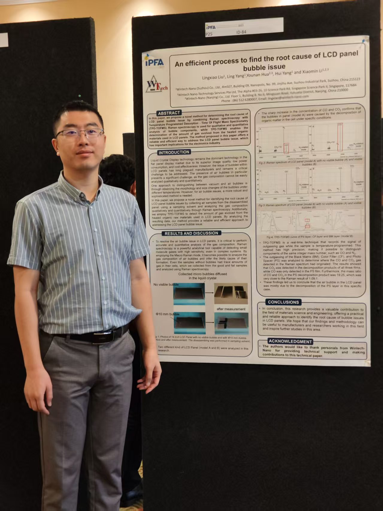
Lingxiao Liu
Senior Technical Manager of Wintech Nano (Suzhou) Co., Ltd.
The 7th CHInano Analysis & Testing Application Forum
Speaker
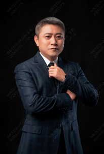
Xiaomin Li
Chairman of Wintech Nano (Suzhou) Co., Ltd.
This report delves into the cyclical development trends emerging in the analytical testing field against the backdrop of rapid iteration of semiconductor technology. It points out that the core of future industry competition lies in technological innovation and specialized division of labor, and systematically elaborates on how the "Labless" business model, as a key driving force, can effectively support R&D and optimize the industrial ecosystem. At the practical level, it proposes a "sector rotation" strategy to dynamically align with R&D investment trends, while explaining the "Lab-Lite" collaborative model that aims to comprehensively enhance supply chain resilience and R&D efficiency through close collaboration between in-house corporate laboratories and third-party laboratories, thereby achieving sustainable development.
Li Xiaomin, Chairman of Wintech Nano, held a Bachelor's degree from Peking University and a Master's degree from National University of Singapore. He has applied for numerous invention patents and published over 100 papers and co-authored two books. In 2001, Li Xiaomin worked at the Agency for Science, Technology and Research (A*STAR) in Singapore. In 2004, he founded WinTech Nano-Technology Services Pte. Ltd. in Singapore, and in 2012, he established Wintech Nano (Suzhou) Co., Ltd. Under his leadership, the company has become a renowned platform for semiconductor chip analysis and testing services, as well as a crucial support center for R&D in the industry. Li Xiaomin introduced the innovative "Labless" concept, which involves outsourcing the "necessary but non-core" R&D segments from the industry, creating a new independent sector.
The 7th CHInano Analysis & Testing Application Forum
Speaker
Yi Zeng
Director of the Testing Center at the Shanghai Institute of Ceramics, Chinese Academy of Sciences (SICCAS)
Scanning electron microscope (SEM), as a common means of microstructural analysis, is often used by many people merely as a "magnifying glass with higher magnification" and generally believed to provided limited scientific information. This report will, by sharing examples, demonstrate how to use the microstructural information obtained from SEM to scientifically interpret the influence of the thermal shock resistance performance of thermal barrier coating (TBC) materials and the high-temperature molten salt corrosion resistance performance of environmental barrier coating (EBC) materials, developing new mechanisms through the interpretation of microstructures, which provides direct scientific basis for improving material properties.
Zeng Yi, Research Fellow, Doctoral Supervisor, Director of the Testing Center at the Shanghai Institute of Ceramics, Chinese Academy of Sciences (SICCAS), Director of the Industrial Technology Basic Public Service Platform for Advanced Inorganic Materials Science and Engineering of the Ministry of Industry and Information Technology, and Director of the Shanghai Quality Inspection Center for Key Ceramic Materials and Devices. Mainly engaged in researches related to scanning electron microscopes (SEMs), he serves as the Chief Scientist of the Instrument Development Special Project under the National Key R&D Program and has undertaken a number of national and local scientific research projects as the person in charge, including the Materials Genome Special Project of the National Key R&D Program, the 863 Program, international cooperation projects of the Ministry of Science and Technology, and Shanghai Science and Technology Support Program. He has published more than 100 SCI papers as the first author or corresponding author. He also holds positions such as Standing Director of the Chinese Electron Microscopy Society, Deputy Director of the Scanning Electron Microscope Professional Committee of the Chinese Society for Electron Microscopy, and Vice President of the Shanghai Society for Microscopy.
The 7th CHInano Analysis & Testing Application Forum
Speaker
Yunyu Wang
Chairman of Xiamen Yunmao Technology Co., Ltd.
In cutting-edge fields, advances in material performance rely on Atomic manufacturing technology. Yunmao Technology utilizes high-vacuum PEALD as its core approach, combining self-limiting reactions and ultra-high vacuum conditions to achieve exceptional thin-film purity and uniformity, meeting the cryogenic processing demands of quantum devices. Its specialized low-oxygen deposition technique minimizes oxygen content, providing critical support for key quantum infrastructure such as ultra-low-loss RF circuits and TSV filling. Thermal ALD also delivers superior conformality for novel nanomaterials. Through continuous innovation, Yunmao is offering essential technical support and critical material solutions for cutting edge industries.
Dr. YUNYU WANG, Founder and Chairman of the Board of Xiamen Yunmao Technology Co., Ltd., holds a bachelor's degree from Nankai University, a Master's and a PhD in Physics from North Carolina State University, and conducted postdoctoral research at the University of Texas at Austin, specializing in the growth, characterization, and application of nanomaterials. He has published over 30 SCI papers (with citations exceeding 1,000) and holds 11 international patents. With over 20 years of experience in high-end equipment product and process development, he previously the developed products such as HDPCVD and Selective Etch etc.
The 7th CHInano Analysis & Testing Application Forum
Speaker
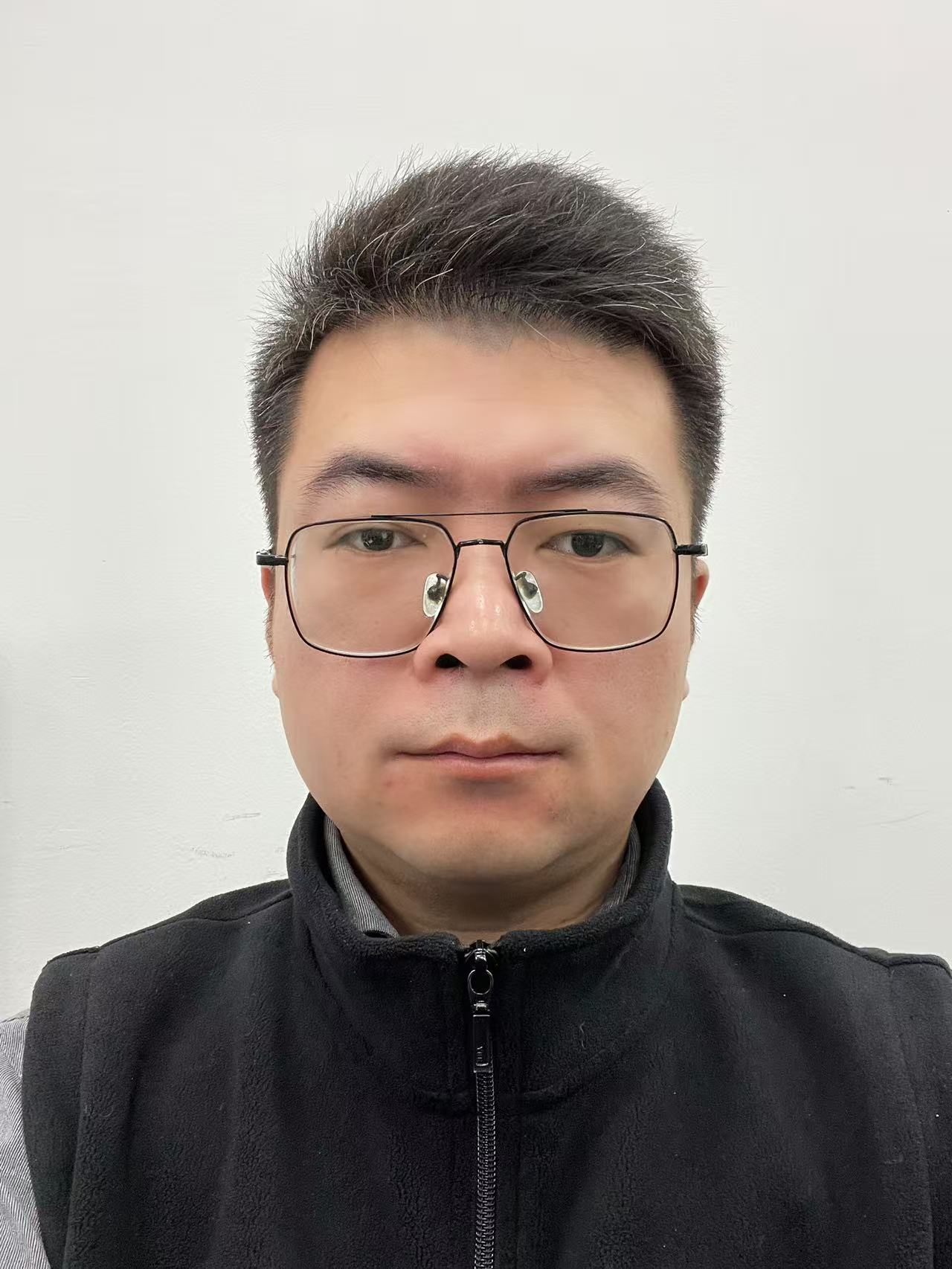
Linhua Zhang
Deputy Technical Director of Wintech Nano (Suzhou) Co., Ltd.
As Moore's Law approaches its physical limits, 3D packaging technology has become a core driver for advancing high-performance computing, artificial intelligence, and 5G communications. However, ensuring reliability under high-density integration has emerged as an unprecedented severe challenge. This presentation will conduct an in-depth analysis of the 3D packaging ecosystem—covering everything from the technical principles of 3D packaging to chip failure analysis technologies—and will use practical cases to elaborate on the diagnostic ideas and solutions for complex system-level faults.
Linhua Zhang, majored in Electronic Information Engineering, previously working in the Laboratory of Changjiang Electronics Technology Co., Ltd. and Integrated Service Technology Co., Ltd., was responsible for comprehensive analysis experiments at the package level and chip level. He has more than ten years's experience in laboratory management and application. Currently, he holds the position of Technical Deputy Director of Comprehensive Analysis Department at Wintech Nano (Suzhou) Co., Ltd., where his responsibilities include, but not limited to, providing technical support for failure analysis of semiconductor devices such as integrated circuit (IC) chips, optical devices, discrete devices, and MEMS, as well as tackling experimental difficulties. He leads multiple key technical research projects for major clients and assists in advancing the R&D progress of clients' new products. During his service, he has participated in and led the drafting and filing of multiple patents, represented by A Localization Method and Device for 3D Stacked Packaging Devices Failure and A Failure Analysis Method for High-Level Chips. He has also published multiple papers at various international conferences, such as Studies and Application of Failure Analysis Technology for Semiconductor Advanced Processes.
The 7th CHInano Analysis & Testing Application Forum
Speaker
Michael Rauscher & Pierre-Yves Guittet
Sr. Director/GM SEM & FIB Product Lines | Semiconductor Business Unit of ThermoFisher Scientific / Director of Product Management and Marketing of ThermoFisher Scientific
Michael Rauscher serves as Senior Product Director for Focused Ion Beam (FIB) Product Line at Thermo Fisher Scientific. He holds a PhD in Ion Beam Physics and has previously held positions in market strategy and product lifecycle management at internationally renowned instrumentation and semiconductor companies, with over 20 years of experience in product management. Pierre-Yves Guittet is Product Director for Transmission Electron Microscopes (TEM) at Thermo Fisher Scientific and has previously responsible for Overlay applications and product marketing at ASML and Nanometrics
The 7th CHInano Analysis & Testing Application Forum
Speaker
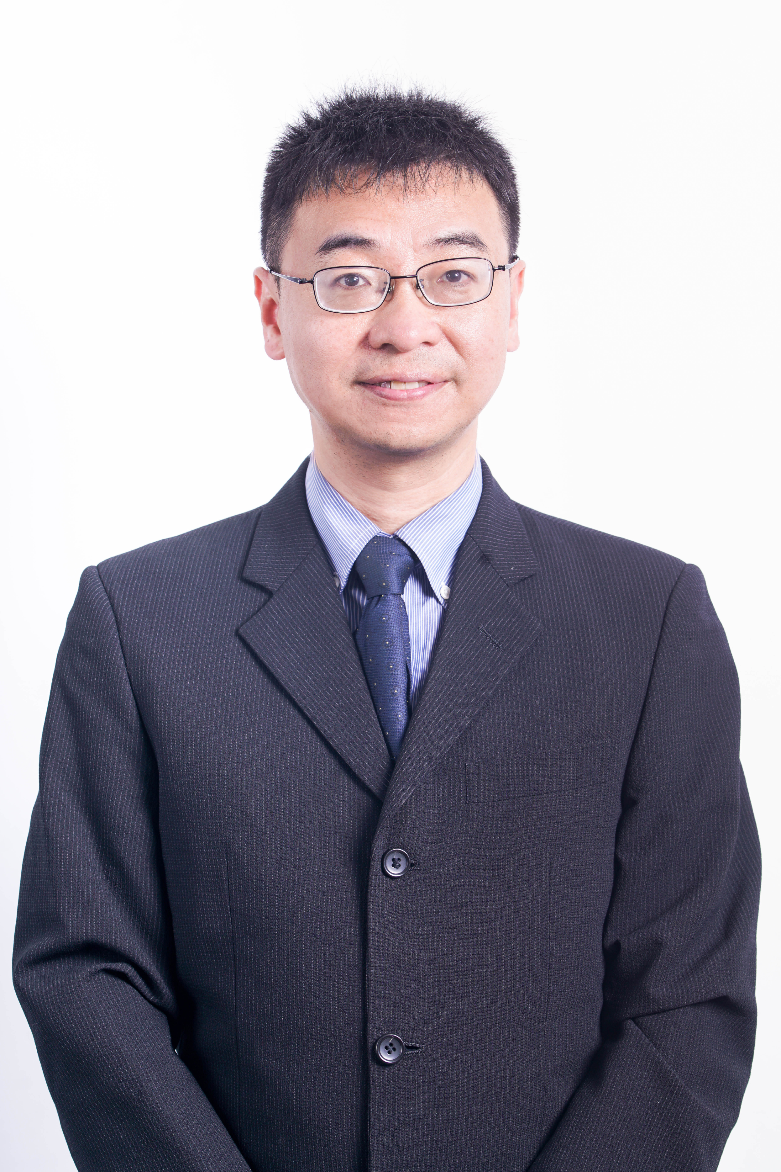
Younan Hua
VP of WinTech Nano-Technology Services Pte Ltd. / DGM of Wintech-Nano (Nanjing)Co., Ltd.
Abstract of Speech:In the integrated circuit wafer fabrication, the quality control of aluminum bondpads in the back-end process is very important. Because no matter what kind of advanced process and how high the yield of wafer fabrication is, as long as the quality of aluminum bondpads on the wafer is not good, the wire cannot be bonded during packaging and problems such as non-bondability occur, the comprehensive yield after packaging will be lower or even zero. At present, there is no standard detection method in the industry to evaluate the quality of aluminum bondpads on wafers. In this report, we will propose a standard OSAT detection method. This method combines the application of Optical microscope, Scanning electron microscope, Auger electron spectroscopy and Transmission electron microscope to characterize and analyze the failure of the quality of aluminum bondpads on IC wafers. If the analysis results meet the predetermined OSAT requirements, it can be qualified that the quality of the aluminum bondpads is good, so that the subsequent packaging process is safe with high-yield. In the report, we will demonstrate several practical application examples of OSAT standard method.
Biography of the Speaker:Dr. Hua received a Ph.D. degree in Physics from National University of Singapore in 1994. After that he worked in Chartered Semiconductor (Globalfoundries), which is a major international wafer fab, and served as Director of Failure Analysis Lab in 1995--2013. In 2014, he joined Wintech-Nano (Singapore) as Vice President/COO. He is an expert in semiconductor wafer fab, process and device failure analysis. He has published more than 400 papers/patents. He has deep academic attainments in the field of wafer fab, packaging and failure analysis, especially in the front-end process of wafer fab, research and development of GOI failure analysis methods and the advanced fab process of anti-pollution and corrosion on Al Bondpads in the back-end wafer fab process with the international leading level. Dr Hua is also actively engaged in and caring about education, and is assigned as a member of the Educational Advisory Committee in National University of Singapore and a PhD Supervisor at National University of Singapore/Nanyang Technological University /Singapore University of Technology and Design / Singapore Economic Development Board / Wintech-Nano (IPP). He also actively participated in the establishment of the Wintech-Nano Semiconductor Institute (WTSI) and served as a Senior Fellow in cooperating with the Singapore University of Technology and Design (SUTD) to jointly train master students in IC design, failure analysis and reliability analysis.
The 7th CHInano Analysis & Testing Application Forum
Speaker
Sarah Ma
Application Scientist of Oxford Instruments Technology China
Abstract of Speech:EDS is a commonly used method in semiconductor failure analysis, but it can only reveal elemental abnormalities. To analyze other physical properties of a wafer (such as roughness, doping concentration, electric potential, and residual stress, etc.), it is necessary to employ Electron Backscatter Diffraction (EBSD), Atomic Force Microscopy (AFM), and Raman Spectroscopy for a multi-scale and multi-faceted detection and analysis. This report will combine semiconductor processes to introduce the advancements in Oxford Instruments' imaging and analytical technologies and their applications in semiconductors, providing more comprehensive failure analysis and R&D solutions from structural, elemental, and physical property perspectives.
Biography of the Speaker:Sarah Ma obtained his Ph.D. in Material Science and Engineering in 2012 from Shanghai Jiaotong University, where she worked on development and characterization of high strength and ductile magnesium alloys. She then completed her postdoctoral work at National Institute of Material Science (NIMS, Japan) and there her major research was characterization of magnesium and magnetic material using HAADF-STEM and 3DAP. After joining in Oxford Instrument as application scientist in 2016, she mainly focuses on application support of Imaging and Material Analysis.
The 7th CHInano Analysis & Testing Application Forum
Speaker
Ou Zhou
Deputy General Manager of Marketing of Hitachi High-Tech Scientific Solutions (Beijing) Co., Ltd.
Abstract of Speech:Since Hitachi developed the electron microscope from 1941, it has developed a variety of different products in various technical directions, including different electron beam emission methods, lens types, ultra-high voltage TEM, etc. Among them, the in-lens SEM is one of the distinctive representative products, bringing ultra-high resolution capabilities and high-speed observation capabilities to semiconductor customers. Today, Hitachi has developed a brand-new in-lens SEM based on the previous generation SU9000II, aiming to meet the continuously rising observation requirements of customers in semiconductor and other fields. At the same time, Nanoprober is playing an increasingly important role in semiconductor failure analysis. EBAC failure site localization is an important function of it. However, EBAC/EBIC and other signals are complex and diverse. How to extract valuable target signals from them is an urgent problem to be solved. For this reason, Hitachi has recently released the Lock-in EBAC function.
Biography of the Speaker:English: Mr. Zhou Ou graduated from Shanghai Jiaotong University. During the master period, he was engaged in the research of transmission electron microscope and semiconductor materials. After graduation, he joined Shanghai Grace Semiconductor, worked in failure analysis lab for many years, and accumulated plenty of application experience of various electron microscope in the semiconductor field. Then he worked in European and American instrument companies for many years, further expanding the understanding of electron microscope application in many industries. Now he is the vice general manager of marketing department of Hitachi High-Tech Scientific Solutions (Beijing) Co. Ltd, mainly responsible for the promotion and technical support of electron microscope series products in the semiconductor industry.
The 7th CHInano Analysis & Testing Application Forum
Speaker
Fenghao Zhong
Deputy General Manager of Hangzhou Changchuan Technology Co., Ltd.
Abstract of Speech:With the increasing demand for chip computing power, high-power logic chips puts forward higher and higher requirements for multi-die integration based on advanced packaging technologies, and their integration level and packaging size are constantly pushing the limits. This has also posed new challenges to testing technologies and test equipment: significant changes have occurred in test processes, test efficiency, test stress, test temperature, and other aspects compared with conventional testing. This report briefly analyzes the challenges brought by multi-die heterogeneous integration to testing, discusses the testing reliability of complex chips, and shares the key technical requirements for test process development and test platform construction.
Biography of the Speaker:Fenghao Zhong, Director, Deputy General Manager, and Senior Engineer of Hangzhou Changchuan Technology Co., Ltd. He has focused on the R&D of integrated circuit (IC) testing equipment for nearly 30 years and is a first-class senior technical expert in the field of IC testing equipment. He also serves as the Leader of the compilation group of Chiplet Testing Standard and an Expert Member of China's National Integrated Circuit Standardization Technical Committee (TC599). He has applied for more than 80 patents related to IC testing technology and published 5 professional papers
The 7th CHInano Analysis & Testing Application Forum
Speaker
Yiming Zheng
Senior Application Manager of ZEISS
Abstract of Speech:Confronted with the dual challenges of high precision and comprehensiveness in failure analysis for advanced semiconductor processes, ZEISS's multi-scale and multi-modal correlative microscopy technology offers an innovative solution. By organically integrating non-destructive and destructive techniques, it successfully implements an advanced analytical paradigm of "Non-destructive First, Precise Correlation, Multi-modal Verification" in fields like advanced nodes, advanced packaging, and third-generation semiconductors. This enables cross-scale defect localization and multi-dimensional failure mechanism analysis, providing robust support for accelerating process development and yield improvement.
Biography of the Speaker:ZhengYiming, Zeiss application manager, he has extensive experience in the semiconductor solutions sector, specializing in the application support of advanced technologies such as Scanning Electron Microscopy (SEM) and Focused Ion Beam (FIB). He is dedicated to delivering key technical solutions for semiconductor materials characterization and failure analysis.
The 7th CHInano Analysis & Testing Application Forum
Speaker
Tim Fai
Application Engineer of Hamamatsu Photonics (China)
Biography of the Speaker:This presentation covers two main topics.In dynamic failure analysis, we will introduce DALS technology for marginal parameter failures (Shmoo), as well as EOP/EOFM technology for frequency response and timing failures (Timing) in IC device layers.In advanced packaging, traditional methods such as OBIRCH and EMMI struggle to effectively detect defects in more complex structures (e.g., BS-PDN). While thermal techniques can identify failure regions through thermal radiation, their operation in the mid-infrared band limits magnification and resolution, making them insufficient for subsequent FIB-SEM analysis. HAMAMATSU's TD Imaging (ThermoDynamic Imaging) technology effectively addresses this challenge, providing a higher-precision failure localization solution.
Abstract of Speech:Currently serving as a failure analysis application engineer, responsible for application training, pre-sales demonstration testing, and post-sales technical support of Hamamatsu's failure localization technologies, providing professional solutions to clients. Previously served as Hamamatsu Stealth Dicing Engine (SDE) after-sales maintenance engineer for China region, acting as the national technical liaison to lead debugging and maintenance of Hamamatsu's optical systems in DISCO stealth dicing equipment, with extensive experience in laser optical processing applications and stealth dicing technical support.
Professional Visitor Registration Entrance Register Now
© 苏州纳米科技发展有限公司版权所有 苏ICP备10213992号-14  技术支持:
全国互联网安全管理服务平台 苏公网安备32059002004852号